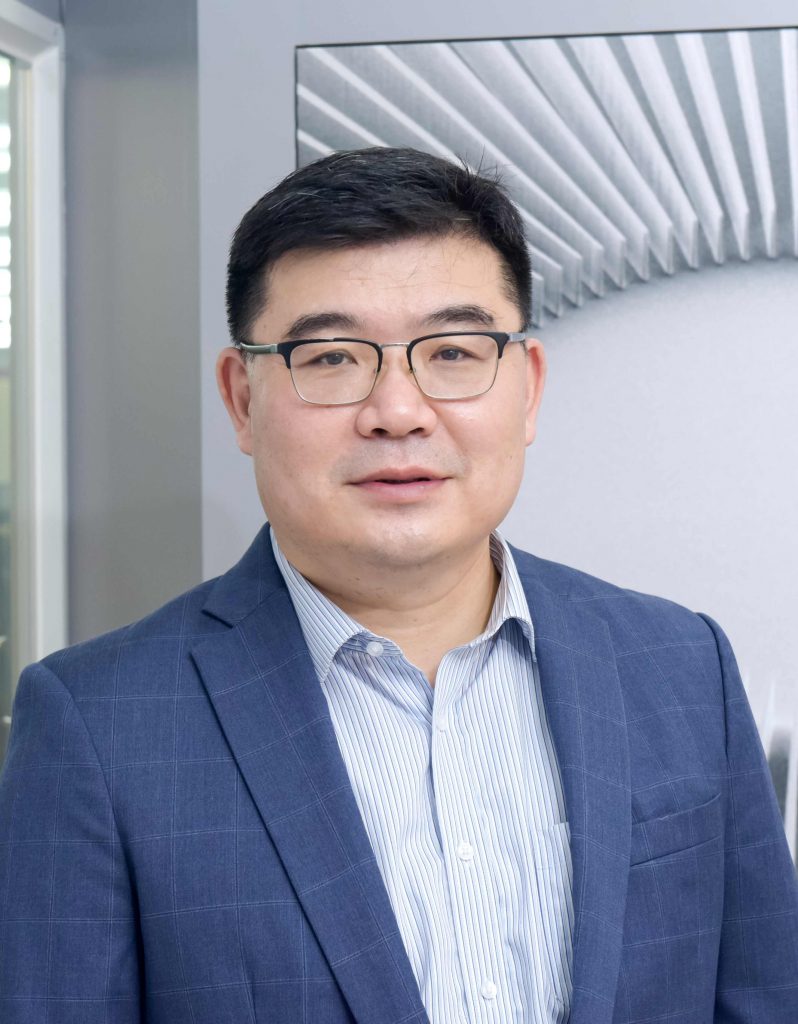
Prof. Chen received a B.S. degree in Department of Electronics, Peking University in 1988. Through the CUSPEA (China-U.S. Physics Examination and Application) program (established by Nobel Laureate in Physics, Prof. T. D. Lee of Columbia University), he went to University of Maryland in 1988, and obtained the PhD degree from University of Maryland, College Park, USA in 1993. From Jan. 1994 to Dec. 1995, he was a research fellow in NTT LSI laboratories, Atsugi, Japan, engaging in the research and development of functional quantum effect devices and heterojunction FET’s (HFET’s). In particular, he developed the device technology for monolithic integration of resonant tunneling diodes and heterojunction FETs on both GaAs and InP substrates, for applications in ultra-high speed signal processing and communication systems. He also developed the buried-Pt gate technology, which is widely used for GaAs-based and InP-based enhancement-mode HEMT and PHEMT implementations. From 1996 to 1998, he was an assistant professor in the Department of Electronic Engineering, City University of Hong Kong, carrying out research on high-speed device and circuit simulations. Dr. Chen then joined the Wireless Semiconductor Division of Agilent Technologies, Inc. (formerly Hewlett-Packard Co.), Santa Clara, California, USA, in 1999 developing RF power amplifiers used in wireless handsets.
Dr. Chen joined HKUST in Nov. 2000, where he is currently a Chair professor in the Department of Electronic and Computer Engineering. He currently serves as the Director of Nanosystem Fabrication Facility (NFF). He is the founding director of InnoHK Power Semiconductors and Applications Center. At HKUST, he established the WIde-bandgap Semiconductor Electronics Laboratory (WISE Lab), focusing on technology development of GaN and SiC power and high-frequency devices and ICs. He has led the invention of novel device concepts including composite-channel III-nitride HEMTs, double-heterojunction and double-channel III-nitride HEMTs, enhancement-mode MISHFETs, planar integration of E/D-mode AlGaN/GaN HEMT, GaN-based MEMS using GaN-on-Patterned-Silicon (GPS) platform, low-density-drain HEMT (LDD-HEMT), lateral field-effect rectifier, metal-2DEG tunnel junction FET (TJ-FET), GaN-on-SOI technology, photonic-ohmic drain FET (PODFET), GaN/SiC hybrid FET, GaN Complementary Logic platform, GaN based non-volatile memory (NVM) devices, dynamic two-stage gate driver for GaN power HEMTs, 3D Co-packaged GaN/SiC cascode devices and associated protection/drive cirtuits. For these inventions, 25 patents have been granted.
His group has also developed many advanced processing including fluorine plasma treatment and implantation, PEALD-AlN passivation, nitridation interlayer and LPCVD-SiN with interfacial protection layer, surface reinforcement technique based on plasma oxidation and surface reconstruction, etc. His group proposed and demonstrated the GaN smart power IC technology for intelligent high-efficiency power and energy management. He is a pioneer in developing and understanding the fluorine plasma ion implantation technique for enhancement-mode and normally-off AlGaN/GaN HEMTs and MIS-HEMTs. His group has also developed atomistic process modeling and simulation tools for the fluorine plasma ion implantation technology and surface nitridation technology.
Prof. Chen is an IEEE fellow and a JSAP (Japanese Society of Applied Physics) Fellow International. He is also a Hong Kong RGC Senior Research Fellow. He has served as a Distinguished Lecturer for IEEE Electron Devices Society in area of advanced III-nitride technologies. He is a member of IEEE EDS Power Semiconductor Devices and ICs technical committee. Prof. Chen has served as an editor of IEEE Transactions on Electron Devices, IEEE Transactions on Microwave Theory and Technique (T-MTT) and Japanese Journal of Applied Physics.